FLEXIBLE PCB – DESIGN TIPS AND TRICKS
How often is your application requiring an higher degree of liberty like bending and twisting? Flexible PCBs give designers the solution to situations that a rigid PCB could not afford. But flexibles are not indestructible, and they require a specialized good design and material selection to guarantee the reliability of the board.
There are several flexibles requirements that a flex PCB could undergo, for example some applications require a continuous dynamic bending (like laptop monitor) or some other application require that the flex PCB will be folded on itself for space optimization.
All the considerations below will be useful for designing a best-performance flexible PCB.
- START TO UNDERSTAND HOW THE BENDING IS MADE


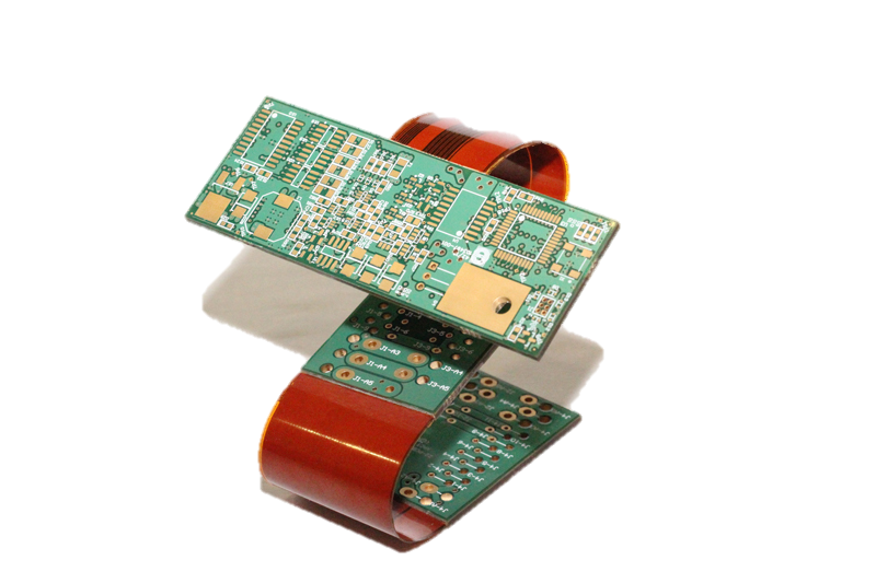
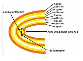
The image above show a flexible PCB and its cross section bent on a tight radius. If the bending radius is too small, the inside of the bend tends to be compressed while the outside tends to extend. If the radius is small enough, the copper layer will fracture.
- COPPER LOCATION AND DYNAMIC BENDING
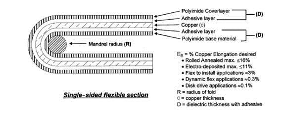
If your application require a dynamic bending PCB, the best solution that you could design is a single side circuit. Whit this specification, the PCB will be a copper foil with dielectric insulation layers evenly distributed in both directions (sides) of copper. With this layup, the copper will be not affected by tension or compression during bending. This particular copper position is called “neutral axis”.
- PCB THICKNESS DILEMMA AND TRACK POSITION
As the bending radius for flexibles PCB is a function of the PCB thickness (see section 4 for detailed calculation, or IPC 2223 for IPC friendly users) consider the golden rule: “thinner is better”. In fact, is normal for a flexible PCB supplier to work with ¼ oz or ½ oz for flex applications.
- PCB BENDING RADIUS CALCULATIONS (IPC-2223 for reference)
For bending radius estimation, for single side flex PCB:


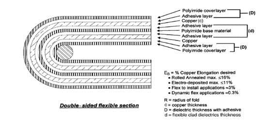
For bending radius estimation, for double side flex PCB:


By inserting in the equation the allowable copper deformation, it’s possible to determine the minimum bending radius.
For reference, you could use these parameters for EB:
For 1-bend PCBs use 16%
For Flex-to-install use 10%
For Dynamic bending use 0.3%
- I-BEAM DESIGN RULE AND 90 DEGREES TRACK TURNS
I-BEAM is the situation that you have when you design tracks that lie into opposite sides of the dielectric layer, directly one over each other. The construction obtained is much more rigid when is placed on a bending area, because of the added thickness of the inside layer.
To avoid this situation, traced should be staggered, like the image below.

For reducing the stress of a onetime fold or a repeated folding and unfolding, and for avoiding cracks in copper foil too, radiused traces are adopted, for reducing the stress along the fold axis. Copper traces width needs to be uniform across bending point and copper tracks size transition should be at least at 0.75mm from the designated bending point.
- SOLDERED CONNECTIONS OR SOLDER PLATED PADS
Solder alloy, during the soldering process, will create an intermetallic bond between the copper and the alloy. This layer is the responsible of the adhesion of the components to the PCB, and is either strong as fragile and could not be bent.
Soldered areas should be kept away from the bending point, and through holes also should be kept at a minimum distance of 1.27mm from the bending point (or in alternative, as a mnemonic rule, should be kept at a distance, from the PTH hole, that is 10 times the PCB thickness).
- COPPER TYPE AND GRAIN DIRECTION
Copper for Flexible application could be divided into:
- Electro deposited copper (ED)
- Rolled and annealed copper (RA)
- High ductility electro deposited copper (HDED)
RA copper should be used for dynamic flexing or for severe folding or bending, as the elongated grain structure of RA copper can withstand more stressing.
Circuits should be placed on the fabrication panel so the grain direction is perpendicular to the bend line.
- STIFFNERS
For applications where there is coverlay on top and a stiffener on the bottom, the coverlay should overlap the end of the stiffener as shown to avoid stress points on the exposed copper.

