Abstract
Conductive anodic filament have been increasing concerning about PCB reliability in the last few years.
To meet miniaturizing needs and satisfy higher performances, a more and more mayor PCB density is forcing PCB design toward closer conductors, smaller pitches, single-ply dielectrics.
Often electrical applications are requested to function in extreme temperature, humidity and voltages environments.
Moreover RoHS legislation advent involves new materials experiencing, introducing different manufacturing conditions such as higher temperatures in assembling processes due to Lead free alloys.
In this scenery materials insulation resistance becomes a crucial factor; to choose a proper laminate in PCB manufacturing process requires more care than in the past.
CAF formation mechanism
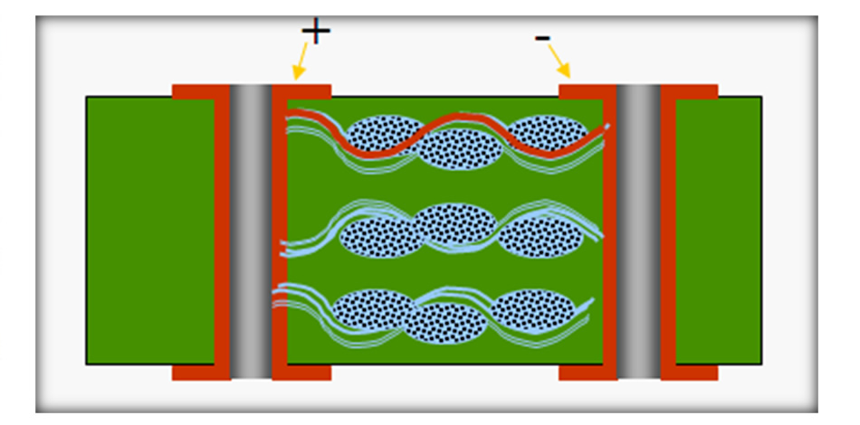
Conductive Anodic Filament consist of a Copper filament growth from a Copper anode to a Copper cathode.
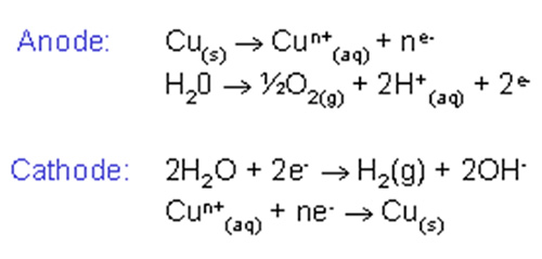
It is due to an electrochemical migration in which Copper ions dissolve through resin/glass fibers interface.
Equation : Electrochemical equation for CAF formation
It depends on:
- circuit layout pattern: spaces between adjacent surface conductors promote CAF
- operating conditions: temperature, humidity, voltage gradient
- substrate material choice: FR4, CEM-3, G-10, MC-2, PI, BT
- laminate quality: humidity absorption and adhesion promoters such as silanes are CAF key factors
- manufacturing processes: lamination, drilling, surface coating
As it leads to current leakage or shorts, it can become responsible of serious field failures.
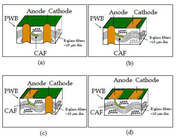
The most common is type (a), as in this case of study, because of the largest surface of contact between Copper barrel and glass fibers
An high density populated multilayer board was taken under examination.
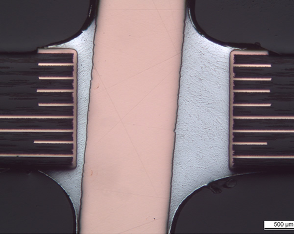
PTH Micro-sections and Scanning Electron Microscope/Energy Dispersive X-ray analysis (SEM/EDS) were the techniques applied to investigate CAF presence.
Results obtained:
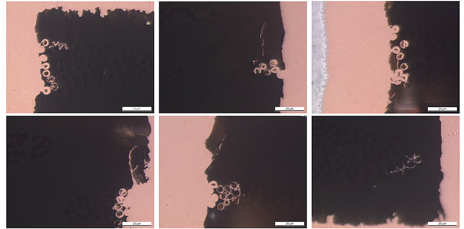
Observing Copper barrel in micro-sections CAF formation was documented in optical microscopy
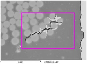
CAF morphology was then characterized by Scanning Electron Microscopy (SEM) secondary and backscattered electrons imaging (SE-BSE)

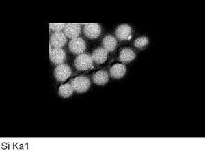
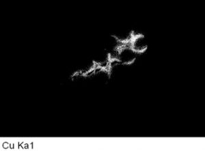
CAF nature was assessed by Energy Dispersive X-Ray microanalysis (EDS)


EDS maps 1: SEM image, glass fibres and Copper filament
Final Statements:
Laboratory analyses are of basilar importance to assess laminates quality and to prevent severe field failures.


